On May 22, 2026 the Department of Commerce announced it had signed nine letters of intent that would provide $2.013 billion in federal incentives under the CHIPS and Science Act, and Bill Frauenhofer of the CHIPS R&D Office framed the move as a targeted, portfolio-driven push to tackle specific engineering barriers across the quantum field.
The paperwork is intended to back two domestic quantum foundry companies and seven quantum computing firms, with the Commerce Department explicitly proposing incentives for GlobalFoundries and IBM as the foundries in the package. The office said the funding is meant to accelerate work on the hardest technical challenges standing between today’s machines and utility-scale, fault-tolerant quantum computers.
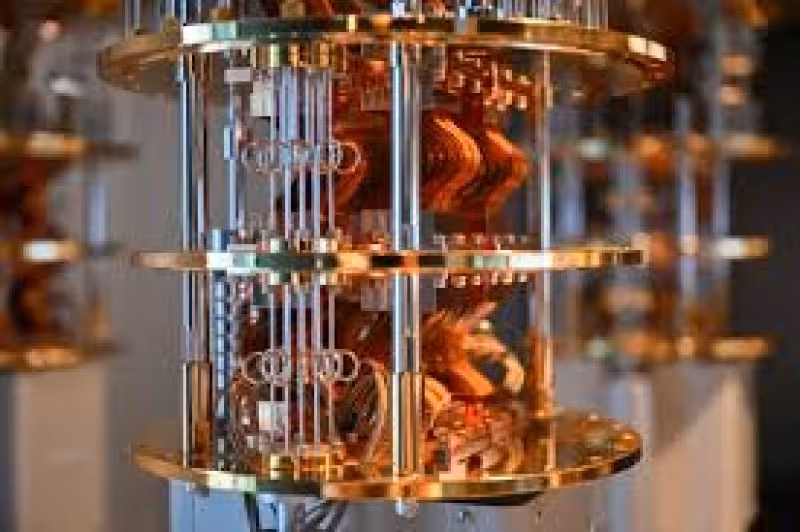
The scale of the announcement is what gives it weight: nine letters of intent and $2.013 billion aimed at both foundry capacity and device-level engineering. The Commerce Department described the portfolio approach as focusing each award on discrete, consequential problems while accelerating multi-year technology roadmaps. Department officials said the incentives will support work across neutral atom, silicon-spin, superconducting, photonic and trapped ion modalities.
Howard Lutnick, commenting on the awards, framed the investments as a political and economic win for the current administration, saying the CHIPS R&D investments will push U.S. innovation forward and bolster domestic industry and jobs. The Commerce Department also emphasized strategic consequences: quantum computing has implications for national defense, advanced materials and biopharmaceutical discovery, financial modeling and energy systems, and the incentive package is presented as a way to strengthen American capabilities in those areas.


Context matters here: the incentives come through the CHIPS and Science Act and are explicitly pitched as research-and-development support rather than finished procurement. The department said the portfolio will attack unresolved engineering problems across multiple modalities — a recognition that no single approach has yet delivered a clear path to scalable, fault-tolerant machines. The announcement pairs foundry-scale proposals for GlobalFoundries and IBM with seven computing-focused projects intended to drive platform-level progress.
The tension in the announcement is plain. These are letters of intent, not final grant awards, and the Commerce Department’s own language stresses the work is intended to solve “the hardest engineering challenges” that remain. That gap — between funding commitments on paper and the messy, multiyear engineering progress required to produce utility-scale, fault-tolerant systems — is where the program will be tested. The portfolio spans neutral atom, silicon-spin, superconducting, photonic and trapped ion technologies, the latter the space where firms such as ionq have concentrated their efforts; the department says the awards will be targeted at problems of genuine consequence within those modalities.
Practically, the next steps are clear: the letters begin a process of negotiations, project designs and milestone-setting between the CHIPS R&D Office and the named parties. The Commerce Department said the incentives will build domestic capacity and speed roadmaps, but deliverables will depend on how quickly participating teams can translate focused R&D dollars into demonstrable advances in error correction, qubit coherence, manufacturing repeatability and integration at scale.
The most consequential question now is whether a $2.013 billion, nine-project portfolio can close the specific engineering gaps that stand between today’s prototypes and the national-security and commercial applications the Commerce Department cited. If the CHIPS-funded awards convert into measured progress on error rates, system size and manufacturability, the program will have justified itself; if not, the letters will read as an expensive experiment in accelerated R&D rather than the decisive leap the announcement promises.